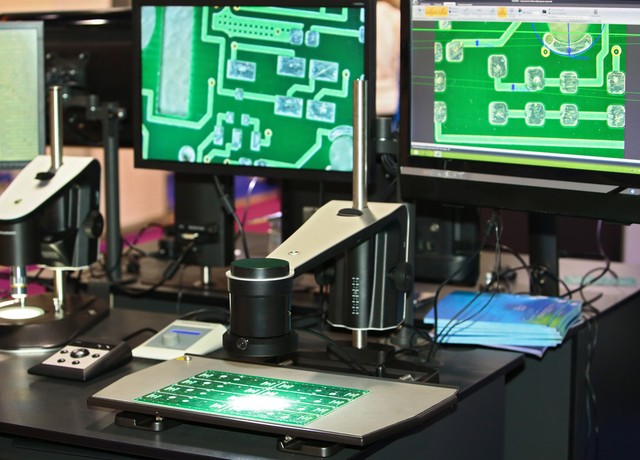
Circuit boards are one of the indispensable components of modern electronic manufacturing. Unlike single-layer circuit boards or double-layer circuit boards, printed multilayer circuit boards have a higher degree of integration and greater signaling capabilities, and can carry up to dozens to millions of components and connecting circuits, which are widely used in computers, communications, medical, aerospace, and other fields.
Printed multilayer circuit board manufacturing companies usually we need to go through several research steps, such as preparing a multilayer circuit for design, drilling, chemical etching, plating and soldering. Among them, the design teaching program of printed multilayer circuit boards supports the entire manufacturing development process and determines its efficient and reliable quality.
The principle of Printed Circuit Board (multilayer pcb fabrication) is to use different copper layers to connect connectors for signal transmission, signal isolation and circuit control. Said copper layers are connected to said copper layers by means of said inner plated holes and said outer connection is realized by means of said through holes. The printed multilayer circuit boards usually have more than 8 layers, and the use of the compact circuit printing technology allows for the expansion of circuit functions, the realization of high-density wiring, and the reduction of product manufacturing scale by changing the copper layers without increasing the thickness of the circuit board.
In the production process of printed multilayer circuit boards, it is necessary to add electrolyte between the different layers to make the copper foil chemically decompose on the intermediate layer (preg) and become a whole. This process is known as mosaicing. After the resin prepreg in the mold is hardened to a solid state by heating pressure, the entire multilayer circuit board is manufactured.
The electronic signals are then tested to ensure the quality and reliability of the circuit boards and to avoid unnecessary loss of material and waste of time. Only after comprehensive and scientific quality and reliability tests can the printed multilayer circuit boards meet the manufacturing standards and quality assurance.
In order to meet the needs of different customers, the design and manufacture of printed multilayer circuit boards need to strictly follow a variety of quality management system standards and “Reason for Adverse Event Analysis” and other specifications, in order to improve the reliability of the product manufacturing, reduce costs, shorten the manufacturing cycle, to ensure that the performance of the product stability.
Printed multilayer circuit board is a complex manufacturing development process, but it is through the ever-changing copper layer to expand the circuit system functions and high-density wiring, to achieve efficient electronic information transmission, and greatly improve the integration of enterprise products and performance stability. Because of the high efficiency and reliability of printed wiring, PCB factory it can already become a necessity in our electronic equipment manufacturing industry, widely used in various different fields and industries in society, is one of the most important components of modern agricultural electronic data technology issues.
相關文章:
